


The combination of high nucleation rate and low growth rate in pulsed plasma produced in liquid media, allowed to synthesize indium nanoparticles encapsulated supposedly in graphene nanoribbons. This paper presents the results of identification of indium nanoparticles obtained in hexane, by X-ray analysis, electron microscopy and Raman spectroscopy.
Keywords: pulsed plasma, indium nanoparticles, liquid media,electron microscopy, Raman spectroscopy.
1. Introduction
Indium — an element of group III of the periodic system with a low melting point (156 0С), superconductor with critical temperature 3,41 K [1].
The indium nanoparticles have an active plasmon resonance [2], could also be used for single electron transit tors, as tags for detection of DNA hybridization, as printing building blocks in nanoxerography, and as starting material for convenient synthesis of InP using phosphide ions [3].
It has been reported [1] about simple and effective synthetic method to prepare monodisperse indium metal nanoparticles less than 10 nm in size by lithium borohydride reduction in amine based solvents, reduction of InCl by alkalides [4]. A one-step, economical nanoemulsion method has been introduced to synthesize low-melting-point metallic nanoparticles. This nanoemulsion technique exploits the extremely high shear rates generated
by the ultrasonic agitation and the relatively large viscosity of the continuous phase — polyalphaolefin (PAO), to rupture the molten metal down to diameter below 100 nm [5]. These listed methods allow obtaining the synthesis of indium nanoparticles of different dispersity, i.e. with different physicochemical properties.
The most common kinetic regularities of formation of nanoparticles are a combination of high nucleation rate of the crystalline phase at a low rate of growth. This is the natural character of our proposed method for the synthesis of indium nanoparticles using the energy of pulsed plasma produced in liquid media [6–10].
2. Method
The experimental setup for pulsed plasma in liquid (PPL) consisted of two main components: a low voltage alternating current electric power supply and a reactor including an anode and cathode, as shown in Fig. 1.
Method is very simple and does not require vacuum system, high- energy, cooling system, but can evaporate even refractory metals. Energy of a single impulse is controlled by changing the capacitance of the capacitors.
Impulse discharge arises between the two electrodes when they are brought close to each other and causes dispersion of the electrode material. By changing the parameters of the discharge circuit (voltage, current, impulse frequency and capacitor capacitance), destruction rate of the electrode materials can be controlled.
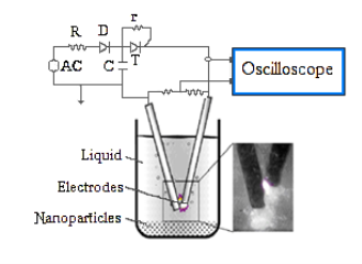
Fig. Schematics of the apparatus used for PPL method.
Quantity of the destroyed material is proportional to the individual impulses energy:
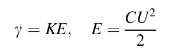 ,
,
where K is proportionality coefficient; E is charged energy in the capacity in Joules, C is the capacity capacitance; U is the charging voltage.
It should be noted that it is possible to synthesize different nanomaterials by changing the electrode materials and the composition of medium [7].
In this studyin order to obtain nanoparticles of indium impulse plasma with single-pulse duration of about 3–5 μs were applied between two indium rods submerged in hexane. Continuous vibration allowed maintenance of the pulsed plasma regardless of increasing rods' distance due to the consumption of the rods' indium.
3. Experimental
For indium dispersion by PPL, two electrodes made from pure indium rods were placed inside a beaker, which contains 50 mL hexane. During the process, pulsed plasma was observed between the tips of two rods and the color of the liquid turned dark gradually. The dark powder at the bottom of the reactor were carefully separated by centrifugation from the liquid and washed with ethanol and dried at room temperature for 1 hour in a desiccator, purged with helium.
The X-Ray Diffraction (XRD) patterns were obtained using the powder method by Rigaku Geigerflex X-Ray Diffractometer RINT 2500 using Cu Kα radiation (Kumamoto University, Japan).
The electron diffraction patterns of the products were taken by Transmission Electron Microscopy (TEM) JEOL-200FX (Kumamoto University, Japan) and JEOL JEM-1400 (CNBM, Adam Mickiewicz University, Poland): powders were suspended in methanol and ethanol and stirred by ultrasonic treatment to disperse the nanoparticles at the room temperature prior to the TEM analyses. Then the particles were dropped onto copper grids covered with carbon film and dried in the air for TEM observations.
Nanoparticles of indium by PPL were analyzed by Renishow inVia Raman microscope (CNBM, Adam Mickiewicz University, Poland).
4. Results and Discussion
4.1. XRD, TEM and Raman spectroscopy analyses.
The analyses of XRD shown in Fig.1 allowed to establish the formation in hexane of indium particles with face-centered tetragonal lattice (а = 0, 323 нм, с = 0, 495 нм, z = 2, space group 14/mmm).

Fig.1. XRD patterns of indium dispersion in hexane by PPL
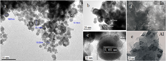
Fig.2. TEM picture of indium and aluminum nanoparticles by PPL
The morphology and size of indium particles were imaged using the Transmission
Electron Microscopy (TEM) JEOL-200FX and JEOL-120FX.
On the TEM-picture (JEOL-120FX) (Fig.2, a, b, c) visible size received in CNBM indium nanoparticles is 10–23 nm. No clear lattice fringes could be observed, and this was attributed to the particles being in a molten state as a result of interaction with the electron beam in the TEM (Fig.2, b — the arrow shows the molten nanoparticles). After much effort, we still managed to take a picture, which shows value close to the parameter of the crystal lattice c of indium nanoparticles– 0, 481 nm (Fig.2, c). Decreasing of the lattice parameter can be attributed to the presence of compressive stresses through a carbon membrane on the surface of indium nanoparticles, which clearly shows on the surfaces of nanoparticle of indium (Fig.2, c — shown by arrows).
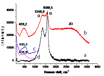
Fig.3. Raman spectra of indium nanoparticles by PPL.
To clarify of the membrane nature were removed Raman spectra of freshly indium nanoparticles (Fig.3, a) and of the same sample in one week (Fig.3, b). According to Raman spectroscopy in the spectra of freshly nanoparticles are two major peaks: G-line, characterized by fluctuations of sp2 carbon bonds (~ 1588 cm -1) (graphite-zone), as well as it is believed that the appearance of D-line (~ 1348 cm -1) indicates the formation of defect structure with respect to graphite or the finite particle-size effect [11,12]. The appearance of nanostructures differ from graphite can be clearly seen on the TEM (JEOL-200FX) images of indium (Fig. 1, d) and aluminum (Fig. 1. e) nanoparticles obtained in hexane. It can be seen that the nanoparticles of indium and aluminum tape wrapped in carbon nanostructures (nanoribbons possible).
Next Raman spectrum of indium nanoparticles from hexane after storage for a week was obtained (Fig.3, b). You may notice that the intensity of the D- line increases, there are two rounded peaks in the 469 cm -1 and 2300–3500 cm-1. Increasing of intensity of D-peak is attributed to the increase in the number of defects in the carbon, which in turn is due to the advent of planar carbon nanostructures. According to the literature, in addition to the bands of the first order, some combination of bands located at 2694, 2937 and 3150 cm- 1 (2D-region)
[13] can also be observed in the Raman spectra and decrease relate to the number of layers in the tape carbon nanostructure. All this is confirmed by the appearance of the peak in the 469 cm -1, which we attributed to the nanoparticles of indium, which probably were bare, thanks to the «unwinding» of tape to form nanostructures of planar systems. To clarify the position of the peak 469 cm-1 Raman spectrum of massive indium and indium nanoparticles without carbon shell synthesized in deionized water was filmed. It can be seen (Fig. 3, c) that the peak of bulk indium (513 cm -1), indium nanoparticles from water (431 cm- 1) (Fig. 3, d) and nanoparticles encapsulated in a carbon (469 cm -1), located in one area. You may notice shift lines of encapsulated indium nanoparticles and nanoparticles from water relative to the massive peak of indium in the shorter wavelengths, which allows us to note the formation of indium nanoparticles in hexane and deionized water, and in water are formed smaller nanoparticles. Calculated size data obtained by Raman spectra shift towards the massive range of indium: of encapsulated nanoparticles 15–35 nm, of nanoparticles of water — 7–13 nm.
Conclusion
Using the pulsed plasma energy produced in hexane by dispersion of indium its tetragonal-packed nanoparticles encapsulated supposedly in graphene ribbons obtained. When storing layers of graphene nanoribbons «unwind», while indium nanoparticles become bare and actively interact with the optical radiation, observed by the Raman spectra.
References:
- T. H. Lim, B. Ingham, K. H. Kamarudin, P. G. Etchegoin and R. D. Tilley. Solution Synthesis of Monodisperse Indium Nanoparticles and Highly Faceted Indium Polyhedra. //Crystal Growth & Design. V. 10. 2010. P.3854–3858.
- N. H. Chou. Chemical synthesis of size- and shape-controlled intermetalic and metal nanocrystals. / Dissertation in Chemistry. 2009. P.75.
- R. A. Ganeev, A. I. Ryasnyanskiy, U. Chakravarty, P. A. Naik, H.Srivastava, M. K. Tiwari, P. D. Gupta. Structural, optical, and nonlinear optical properties of indium nanoparticles prepared by laser ablation. //Appl. Phys. B 86. P. 337–341 (2007). DOI: 10.1007/s00340–006–2526–1.
- K. L. Tsai, J. L. Dye. Nanoscale metal particles by homogeneous reduction with alkalides or electrides. //J. Am. Chem. Soc.1991.113 (5). P. 1650–1652. DOI: 10.1021/ja00005a031.
- Z. H. Han, B. Yang, Y.Qi, J. Cumings. Synthesis of low-melting-point metallic nanoparticles with an ultrasonic nanoemulsion method.//Ultrasonics. 2011. 51. P. 485–488.
- S. Sulaimankulova, E. Omurzak, J. Jasnakunov, A. Abdykerimova, H. Gafforova, A. Mametova. New Preparation Method of Nanocrystalline Materials by Impulse Plasma in Liquid. //J. CLUST. SCI. 2009. V. 20. N1. P. 37–49. DOI:10.1007/s10876–008–0225–2
- S. K. Sulaimankulova, U. A. Asanov. Energy-Saturated Media in the Plasma of Spark Discharge (Kyrgyzpatent, Bishkek, 2002).
- E. Omurzak, T. Mashimo, S. Sulaimankulova, S. Takebe, L. Chen, Zh. Abdullaeva, Ch. Iwamoto, Y. Oishi, H. Ihara, H. Okudera and A. Yoshiasa. Wurtzite-type ZnS nanoparticles by pulsed electric discharge. //Nanotechnology. 2011. V.22. P.365602.
- L.Chen, C. Iwamoto,E.Omurzak,S. Takebe,H. Okudera,A. Yoshiasa,S. Sulaimankulova, T.Mashimo.SynthesisofZirconiumCarbide(ZrC)Nanoparticles CoveredwithGraphitic“Windows”byPulsedPlasmainLiquid. //RSCAdvances. 2011. V.1 (6).P. 1083–1088...
- A. Matkasymova, E. Omurzak, S.Sulaimankulova. Nanorods of Metallic Bismuth and Antimony by the Impulse Plasma in Liquid. //J.Clust.Sci. 2009. V.20. N1. P. 153–158. DOI 10.1007/s10876–008–0230–5.
- A. C. Ferrari, J. Robertson. Resonant raman spectroscopy of disordered, amorphous, and diamond like carbon. // Phys. Rev. B. 2001. V.64 (7). P. 075414–1-13.
- M. A. Pimenta, G. Dresselhaus, M. S. Dresselhaus, L. G. Cancado, A. Jorio, R.Saito. Studying disorder in graphite-based systems by Raman spectroscopy. //Phys. Chem. Chem. Phys. 2007.V.9. P. 1276–1291.
- P. Tan, S.Dimovski, Y. Gogotsi. Raman scattering of non-planar graphite: arched edges, polyhedral crystals, whiskers and cones. //Philosophical Transactions of the Royal Society A. 2004. V. 362. N182. P. 2289–2310.
